統合シリコンフォトニックパッケージ
引用
Hwang, HY (2019). 統合シリコンフォトニックパッケージング[博士論文、University College Cork]. https://hdl.handle.net/10468/9524
キーワード
- シリコンフォトニクス
- パッケージ
- 統合
- 光学アセンブリ
- 電気インターポーザー
- グレーティングカップラー
- エバネッセント結合
- MEMS光スイッチ
簡単な
この論文は、高密度統合とパッシブ光アセンブリに重点を置いた高度なパッケージング技術を開発および実証することにより、シリコンフォトニクスの研究と製造の間のギャップを埋めることを目的としています。
まとめ
How Yuan Hwang 氏 (2019 年) の博士論文「統合シリコン フォトニック パッケージング」では、デバイス製造と最終パッケージ製品の間のギャップを埋めることを目指して、シリコン フォトニクスの高度なパッケージング技術を探求しています。この論文では、シリコン フォトニック パッケージの大量生産を可能にするために、高密度統合と効率的な光結合方法の必要性を強調しています。Hwang 氏は、開発されたパッケージング ソリューションを実証するために、カリフォルニア大学バークレー校の最先端のシリコン フォトニック MEMS 光スイッチをテスト デバイスとして使用しています。
この論文では、シリコン フォトニック デバイスにおける高密度の電気および光相互接続によって生じる課題について取り上げます。2 世代のパッケージング ソリューションが紹介されています。
- 第 1 世代のパッケージングには、電気配線用のセラミック インターポーザと光結合用の蓋なしファイバー アレイを使用した 12x12 シリコン フォトニック MEMS 光スイッチ パッケージが含まれます。このアプローチは、シリコン フォトニクスの 2D パッケージングの実現可能性を実証しています。
- 第 2 世代のパッケージングでは、2 つのテスト車両を使用して高密度の統合を目指しています。
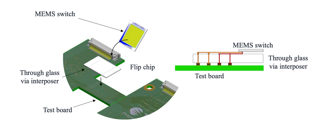
- プラグ可能なパッケージ (テスト車両 2a) は、電気接続用にスプリング接触インターポーザーを備えたセラミックインターポーザーを採用し、光学アセンブリの分離を可能にします。
- ガラス貫通ビア パッケージ (テスト車両 2b) は、2 つのメタライゼーション層と貫通ビアを備えたコンパクトなガラス インターポーザを使用し、電気長を短縮して 2.5D 統合を可能にします。
重要な革新は、イオン交換プロセスを使用して製造された2D、136 チャネル、ピッチ縮小光ファイバー アレイであり、従来のファイバー V 溝アレイの課題に対処しています。この論文では、受動光結合方法についてさらに調査しています。
- 垂直に積み重ねられた格子を使用した格子間結合により、アクティブアライメントが不要になり、2.5D 統合が可能になり、アクティブデバイスのサイズが縮小されてコストが削減されます。
- ガラス貫通ビアインターポーザと統合された埋め込みガラス導波路に基づくエバネッセント結合。この方法により、組み立てプロセスが簡素化され、パッケージングの複雑さが軽減されます。
Hwang 氏は、シリコン フォトニック パッケージの設計ルールと考慮事項を示し、デバイスのレイアウト、材料の選択、およびプロセスの互換性の重要性を強調しています。論文では、パッケージがシリコン フォトニクスの潜在能力を最大限に引き出す上で重要な役割を果たし、革新的なソリューションと、電気的、光学的、熱的、および機械的側面の慎重な統合が必要であると結論付けています。
出典: https://cora.ucc.ie/server/api/core/bitstreams/4c1b8595-1427-4514-bc2f-33c11056d833/content