Design and Demonstration of Glass Panel Embedding for 3D System Packages for Heterogeneous Integration Applications
Citation
Ravichandran, S., Yamada, S., Ogawa, T., Shi, T., Liu, F., Smet, V., Sundaram, V., & Tummala, R. (2019). Design and Demonstration of Glass Panel Embedding for 3D System Packages for Heterogeneous Integration Applications. Journal of Microelectronics and Electronic Packaging, 16(3), 124–135. https://doi.org/10.4071/imaps.930748
Keywords
- Glass Panel Embedding (GPE)
- Heterogeneous Integration
- 3D System Packages (SiP)
- Wafer-Level Fan-Out (WLFO)
- Through Glass Via (TGV)
- Die Shift
- Surface Planarity
- Redistribution Layers (RDL)
- Electrical Performance
- Reliability
Brief
This article presents a 3D packaging technology using glass panel embedding (GPE) for high-performance heterogeneous integration applications. This new technology addresses limitations of current technologies and enables high-density I/O, superior electrical performance, and potential for large body size applications.
Summary
The article, published in 2019 in the Journal of Microelectronics and Electronic Packaging, introduces and demonstrates a novel 3D packaging technology called Glass Panel Embedding (GPE). Authored by Siddharth Ravichandran, Shuhei Yamada, Tomonori Ogawa, Tailong Shi, Fuhan Liu, Vanessa Smet, Venky Sundaram, and Rao Tummala, the article highlights GPE's potential to revolutionize heterogeneous integration in electronic devices.
Here’s a summarized explanation of the article:
- The electronics industry needs advanced packaging technologies for heterogeneous integration, driven by the demand for high performance and power efficiency.
- While Wafer-Level Fan-Out (WLFO) packaging is promising, its reliance on epoxy mold compounds (EMCs) limits its use in large-body applications due to issues like large die shifts, rough surfaces, and moisture absorption.
- In contrast, GPE utilizes glass as a carrier for die embedding, providing several advantages over conventional WLFO with EMC. GPE offers:
- Superior electrical performance: Compared to EMCs, glass exhibits lower loss at higher frequencies, making it suitable for high-speed applications.
- Enhanced design flexibility: Unlike interposers and silicon bridges, GPE is not bump-limited and allows for silicon-like redistribution wiring, increasing I/O density and reducing cost.
- Improved reliability: The tailorable CTE of glass in GPE enhances reliability and allows for direct board attachment, unlike EMC-based packages.
- The article outlines the fabrication process for 3D GPE and details the parametric process improvements implemented to overcome limitations such as die shift and surface planarity issues in traditional WLFO. These improvements include:
- Minimizing die shift to less than 2mm through a novel die-embedding process using a die attach film (DAF).
- Achieving a surface planarity of less than 5mm by optimizing lamination and curing conditions of the dielectric.
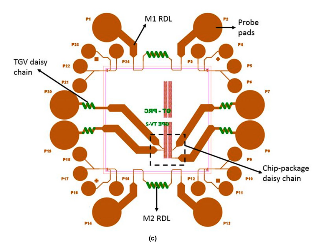
- Successfully integrating through-glass-vias (TGVs) with a 25-mm diameter and 300-mm pitch on 250-mm thin glass panels using a via-in-via approach. This method enhances yield, reliability, and electrical performance.
- The article concludes by emphasizing that 3D GPE, enabled by these advancements, offers a cost-effective, high-density, and high-performance solution for heterogeneous integration.
